Nanocrystals: What are these?
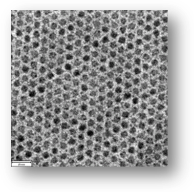 The prefix "nano" stands for 10-9. Particles with dimensions in the nanometer regime are more commonly called nanoparticles in general, nanocrystals in case they are crystalline. Other names such as "quantum dots" have also been suggested for these tiny materials. Typically particles in the size range 2-20 nm exhibit interesting properties and hence it is appropriate to limit the nano nomenclature to such entities. The transmission electron micrograph (TEM) shows an arrangement of self-assembled, 7.7 nm diameter PbSe nanocrystals. PbSe is a semiconductor material. It is possible to synthesize nanoparticles of other types of materials such as metals. Semiconductors are different from metals due to the fact that they have a band gap between the valence band (VB, occupied by electrons) and the conduction band (CB, occupied by holes or in other words empty). Electrons (holes) can be excited from the VB (CB) to the CB (VB) by pumping in appropriate amount of energy into the system. Here, we shall only describe the semiconductor nanocrystals since they exhibit the "quantum confinement effect".
Quantum confinement
 In order to understand quantum confinement, we need to go back to the very basics of quantum mechanics; namely the particle-in-a-box. All we need to worry about is, that the spacings between the energy levels increase as the length of the box decreases. Quantitatively, En = n2h2/8mL2. In the case of semiconductors this simply means that the band gap, starting from the bulk value, increases as the size of the nanocrystal decreases. In bulk solids the energy levels are closely spaced and thus form quasi-continuous bands. Going to the nano-regime the energy level separation increases and discrete energy levels are observed. Calculations on different systems show that quantum confinement effects are observable at sizes below 10 nm for most materials (~20 nm for Pb chalcogenides). Onset of confinement depends on a number of parameters such as the dielectric constant of the semiconductor and effective masses of the charge carriers.
Consequences of quantum confinement
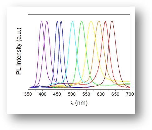 Since the VB-CB transitions are electronic transitions, they occur in the near UV, visible or the near IR region of the electromagnetic spectrum. By choosing different semiconductors, which have different band gaps, it is possible to tune the band gap to be at any energy in this range. The electron that has been excited from the VB to the CB must relax back. If the relaxation occurs radiatively then we have emitters in the entire UV-vis-IR range. One such example is shown in the logo picture. The vials containing solutions of CdSe nanocrystals of different sizes (size increasing on going from left to right) are illuminated by a UV lamp. The fluorescence from these nanocrystals can be tuned all the way between the blue and red regions of the visible spectrum.
Applications
 Fluorescent materials find a large number of applications. A simple example is that of light emitting devices (LEDs). Since nanocrystals absorb all energies higher than their band gap, they can also be used as color converters. Sizes of biological molecules are also on the order of a few nanometers. Tagging nanocrystals to such proteins can help in tracing these biomolecules.
Research Highlights
Layered Double Perovskite: Mn dopingDoping of the transition metal cation Mn2+ in two-dimensional (2D) (PEA)4NaInCl8 (PEA = Phenylethylamine) LDP results in broadband emission at ambient conditions and initial contraction followed by expansion of host lattice on increasing dopant concentration. A higher dopant feed ratio in this wide band-gap material leads to the absorption at 2.95 eV due to the 6A1 (6S ) → 4A1 (4G) transitions on Mn2+ centers. The room-temperature X-band EPR spectra displayed the characteristic sextet pattern at lower dopant concentrations while higher Mn2+ doping leads to merging of the EPR signal into a single broad spectrum implying the formation of Mn2+ cluster due to exchange interaction between magnetically coupled Mn2+ pairs. First-principles calculations based on density functional theory (DFT) confirm that Mn2+ in substitutional sites resulting in lattice contraction while interstitial sites Mn2+ doping leads to lattice expansion. To read more see J. Phys. Chem. C , (2023).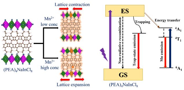
Perovskite StabilityIn this work, stability of 3D halide perovskites (CsPbX3 (X: Br, I)) is tremendously enhanced by growing small islands of PbSe nanoparticles on the surface of perovskite. This is achieved by synthesizing perovskites in presence of MoSe2 nanosheets which acts as the source of selenium. The resulting heterostructure exhibits not only enhanced ambient stability but also improved emission efficiency, owing to the passivation of surface defects of perovskite by PbSe nanoparticles. This work provides an insight about understanding the defect chemistry by tuning the size of one of the components at the interfaces and opens possibilities to further design new class of NHSs to tune their optoelectronic properties. To read more see J. Phys. Chem. C , (2023).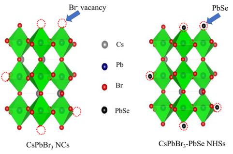
Energy TransferIncorporation of Lanthanide ions (Ln3+) emission in lead-free halide double perovskites is a challenge due to high excitation energy (~250-290 nm) of Ln3+ doped Cs2AgInCl6. Codoping Bi3+(~1%) can induce the emission of Sm3+ at much lower excitation energy in Sm3+-Bi3+ co-doped Cs2AgInCl6 DP nanocrystals (NCs). Spectral analysis shows that trace amount of Bi3+(~1%) doping provides enhanced dual emission of self-trapped excitons (STEs) and four characteristic emissions of Sm3+ assigned to 4G5/2 to 6HJ (J = 5/2, 7/2, 9/2, and 11/2) transitions. luminescence mechanism demonstrated the energy transfer pathway in the synthesized system. Ultrafast transient absorption results confirm the self trapped exciton mediated energy transfer to Sm3+ in these DP nanocrystals. To read more see J. Phys. Chem. C 127, 468 (2023).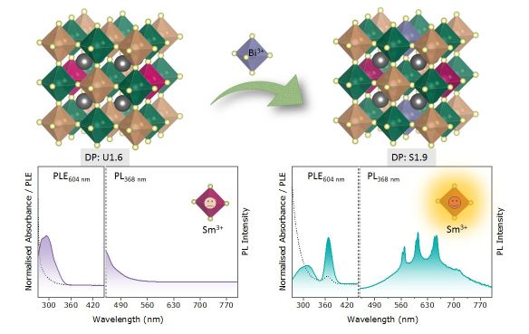
Charge Transfer3D halide perovskites have outstanding optoelectronic properties but still suffer from poor power conversion efficiency. One of the ways to improve their PCE is by designing nanohybrids with suitable counterparts, which enhances the rate of charge transport. II-VI NPLs are good candidates for coupling because of their outstanding optical and transport properties. However, direct growth of CsPbBr3 with CdSe NPLs is difficult because of high lattice mismatch between the two materials. Therefore, the use of bifunctional linker is considered as an effective approach to link these materials. We have used three different bifunctional linkers namely: 4-Aminothiophenol (4-ATP), p-aminobenzoic acid (PABA), and 6-amino-2-napthoic acid (ANA) and study the charge transfer dynamics between the CsPbBr3-CdSe/CdS/ZnS nanohybrids. Both our experimental and theoretical results suggest that efficient charge transfer occurs in case of 4-ATP because of its small size and stronger binding affinity with both constituents, thereby bringing them in close proximity. To read more see J. Phys. Chem. Lett. 13, 2591 (2022). |