Research Areas
Nanoscale Device Engineering
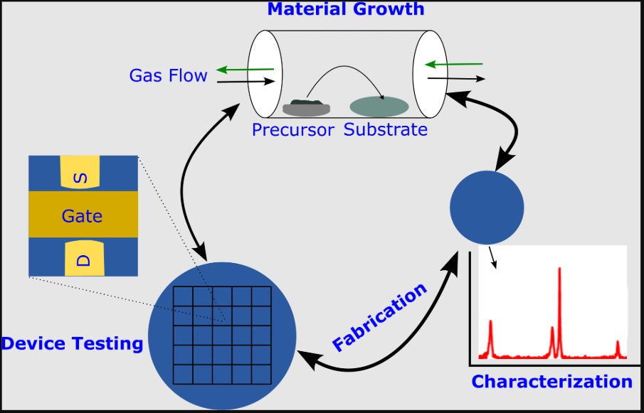
- Synthesis of nanoscale and 2D materials using chemical vapor deposition (CVD) and solution methods
- Interface engineering and heterostructure fabrication
- Electrical and optical characterization of nanoscale devices
- Design and analysis of quantum and nanoelectronic systems
Facilities
Our laboratory is equipped with advanced instrumentation for materials synthesis, device fabrication, and experimental characterization.
CVD Tube Furnace
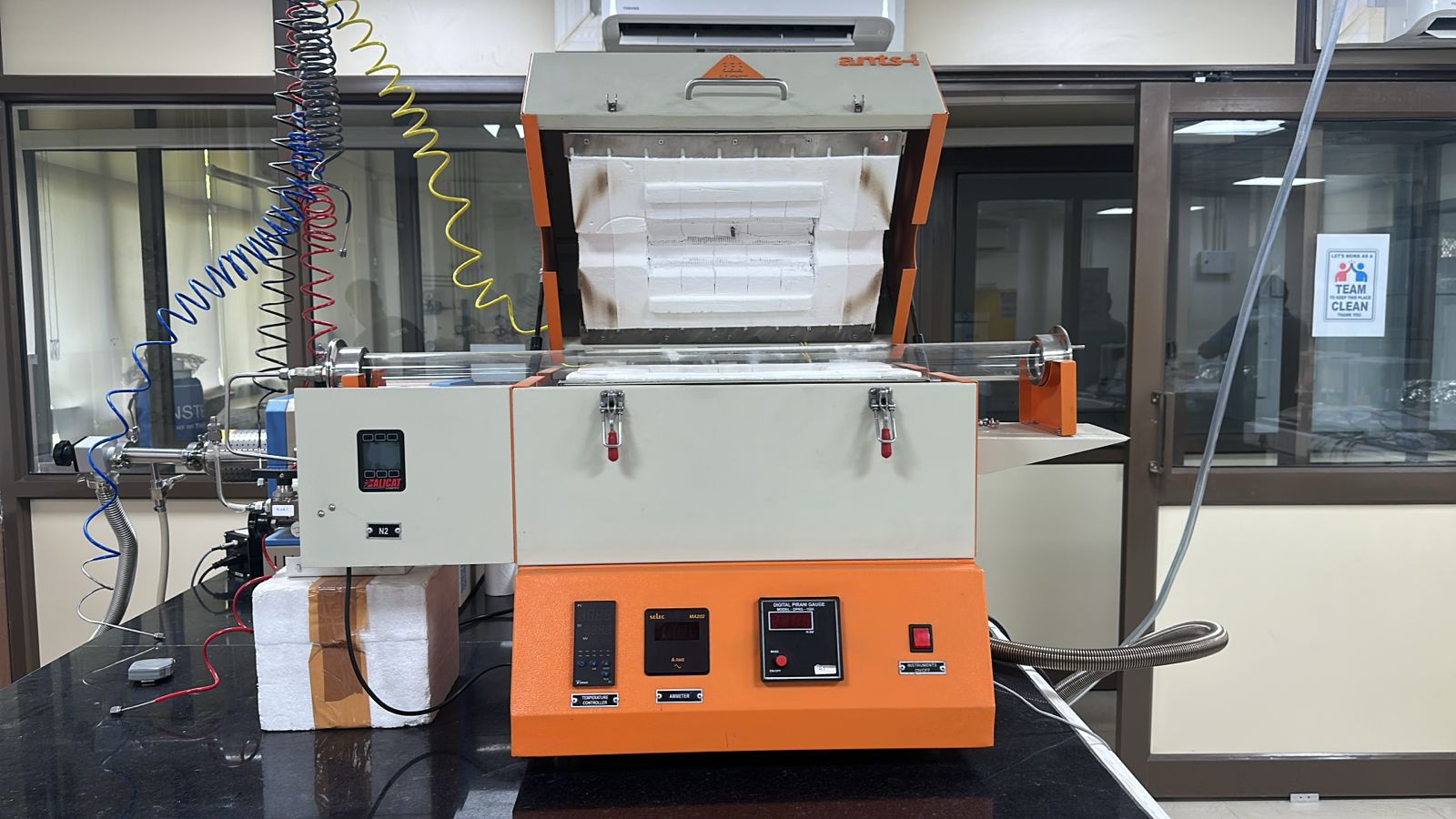
Advanced high-temperature system for thin film deposition and nanomaterial synthesis via Chemical Vapor Deposition.
Microscope
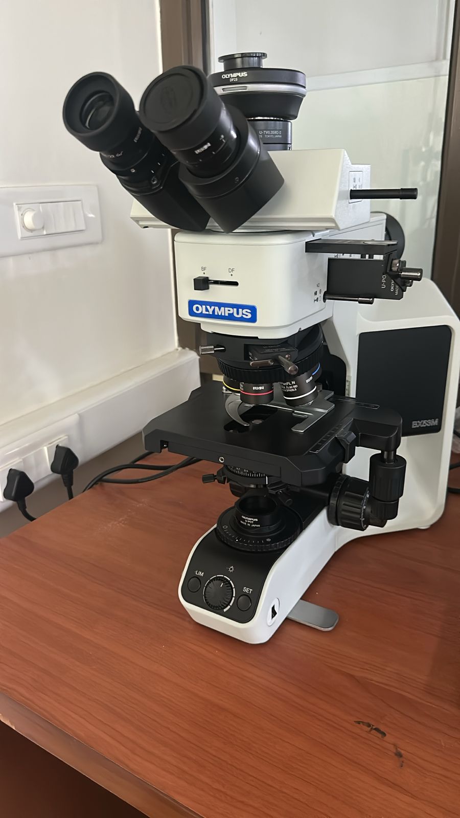
High-resolution optical system used for surface inspection and detailed microstructural analysis of fabricated devices.
Probe Station
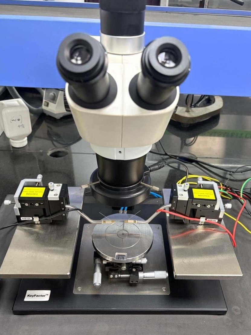
A probe station is a specialized laboratory instrument used to perform precise, microscopic electrical, optical, or RF measurements on semiconductor wafers, dies, or microcircuits.
Research Funding
ANRF
Patterned Native Oxide Dielectrics in 2D Bismuth Oxyselenide for Next-Gen Electronics
Prime Minister Early Career Grant (2025-2028)
Role: PI
IIT Delhi
Start-up Grant
2023–2026
Role: PI
Collaborations
Collaborations with various research groups are actively being developed.
Research Vision
Our research aims to bridge materials science and device engineering to enable next-generation nanoscale technologies with applications in electronics, energy systems, and quantum devices.