
Analog Electronic Circuits
Solutions for practice problems
-
- All NMOS devices VGS is same and 1V, except the device with W/L of 4. Device with W/L of 4 has 0.75 V. All NMOS devices drain current is same and 0.25mA, except tail current source and output NMOS device. Tail current is 0.5mA and output NMOS drain current is 2.8125mA. All PMOS devices has same VSGP 0f 1V and drain current is 0.25 mA except output PMOS device, which has 2.8125 mA.
-
All NMOS devices gm is same and 1mS except W/L=4 device which has 2
mS and tail current source has 2 mS and output NMOS device has 5 mS. All
PMOS devices gm is same and 1mS, except output PMOS device. Output PMOS
device gm is 5 mS.
All NMOS devices gds is same and 20uS except W/L of 4 size device which has 40 uS and tail current source has 40 uS and output NMOS device has 100 uS. All PMOS devices gm is same and 20uS, except output PMOS device. Output PMOS device gm is 100uS.
- Differential DC gain is 2500. CM gain = gm/(1+gm/gds) * (1/gm) * gmro = 0.98 and CMRR is ~ 2500.
- p1=2gds/50Cc , gds is the gds of diff pair MOS and p2=2gm/CL, where gm is the gm of output NMOS. z1=2gm/Cc in right half plane.
- wp1/wp2=tan30/2500 implies wp2=wp1*4.33e3.
- Cc of 1.73 pF.
- R 0f 1kohm is needed in series with Cc.
- UGB=5.8 Grad/sec.
-
- All NMOS devices VGS is same and 1V, except the device with W/L of 4. Device with W/L of 4 has 0.75 V. All NMOS devices drain current is same and 0.25mA, except tail current source and is 0.5mA. All PMOS devices has same VSGP 0f 1V and drain current is 0.25 mA except W/L =2 PMOS devices, which has 0.5 mA.
-
All NMOS devices gm is same and 1mS except W/L of 4 size device which
has 2 mS and tail current source has 2 mS. All PMOS devices gm is same
and 1mS except W/L=2 PMOS devices has a gm of 2mS.
All NMOS devices gds is same and 20uS except W/L of 4 size device which has 40 uS and tail current source has 40 uS. All PMOS devices gm is same and 20uS except W/L =2 PMOS devices and is 40uS.
- Differential DC gain is 625. CM gain is 16.67 and CMRR is 37.5.
- p1=4gds^2/gm/(Cc+CL) and other poles and zeros much far. CL is much larger than the device capacitances on each node in signal path.
- Phase margin of 60 deg is guaranteed with a CL of 5 pF.
- Cc of zero.
- Right half plane zero is much far away from zero
- UGB=gm/CL= 1m/5p = 1/5 G rad/sec.
-
- wp2=wp1*Dcgain/tan(15deg)
- wp2=UGB/tan(90-PM)=373Mrad/sec, wp1=UGB/DCgain=100M/2500=40kHz.
- wp2=gm2/CL=373Mrad/sec, gm2=1.12mS, assuming gm1 is same as gm2. For the Figure 4, gm2 needed is 0.06 mS.
- W/L of the output stage is 1 for all transistors and use half of the current in the figure 4.
-
Possible designs are given below:
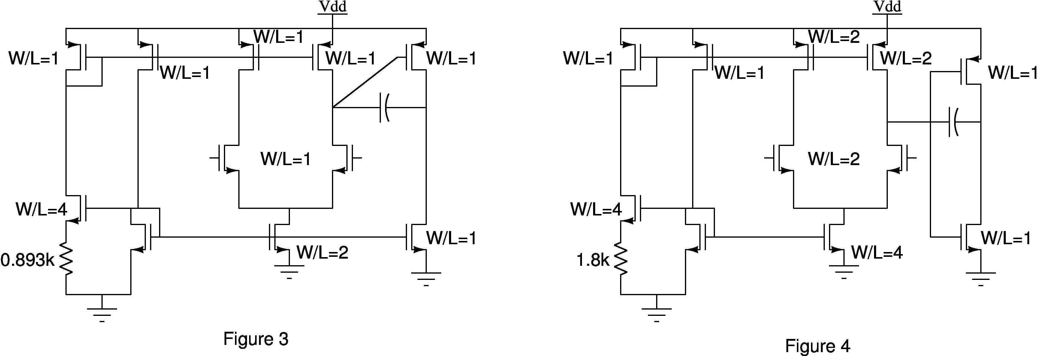
- 4*1.12mA = 4.48mA (Figure 3) and 3.92 mA (Figure 4)
- Approximately doubles.
-
13.1: a. 12.5mA
b. New gain at peak is 0.9577 - 13.3: 7 mW can be delivered.
-
13.8 , 13.16, 13.19 are below.
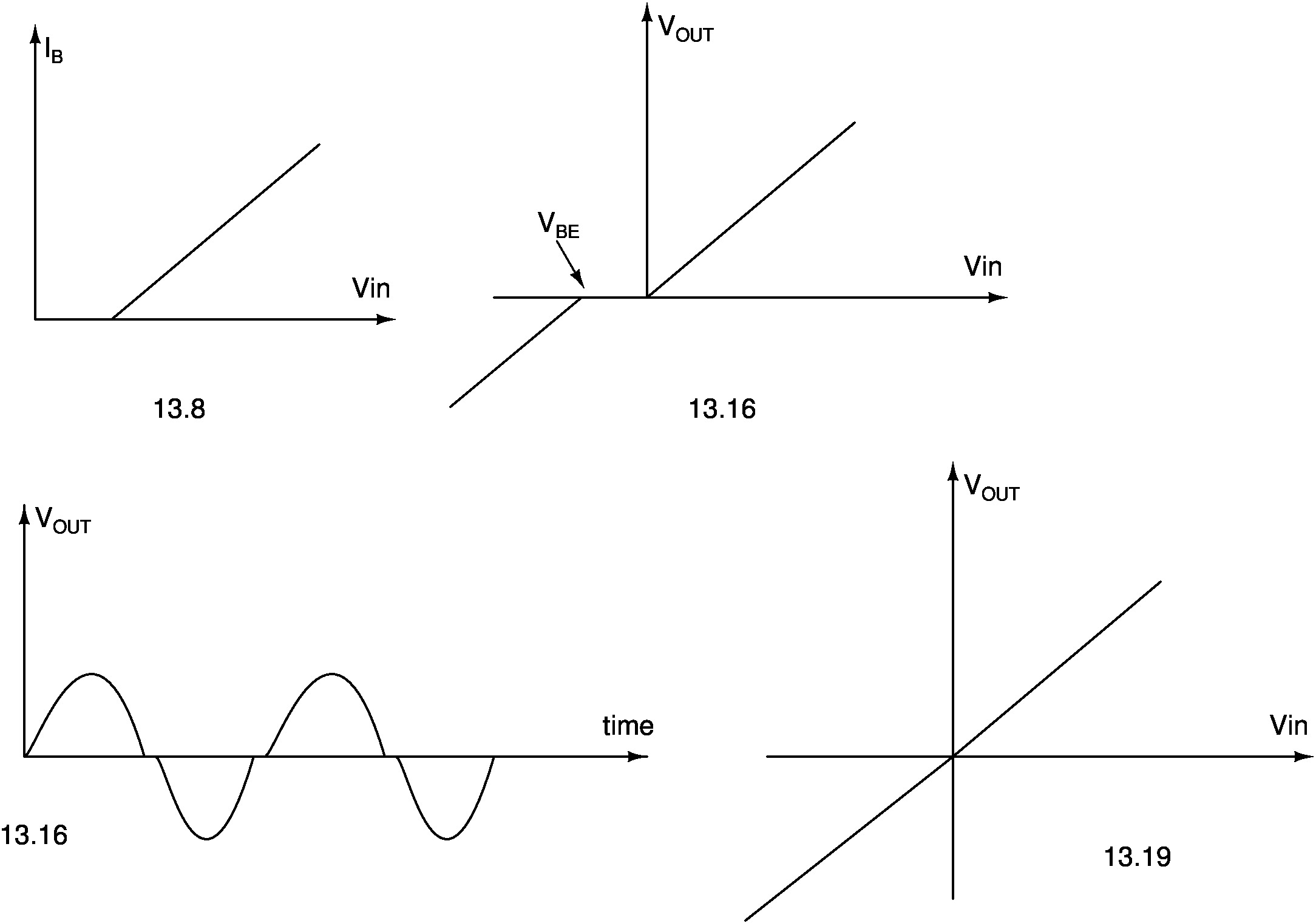
- 13.17 -0.329 V of VB is needed.
 Lectures Lectures |
| Tutorials |
| Venue |
| Laboratory |
| References |
| TAs
|
| Evaluation |
|
Feedback |
| Main |
