Spin and photovoltaic devices
Two-dimensional materials are a unique class of materials with high optical transparency, charge mobility and large spin coherence length. We are looking in novel devices which are formed by interfaces of two-dimensional materials with conventional materials for a variety of spin transport related applications and photovoltaics.
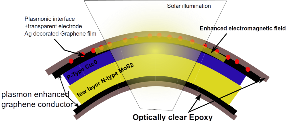
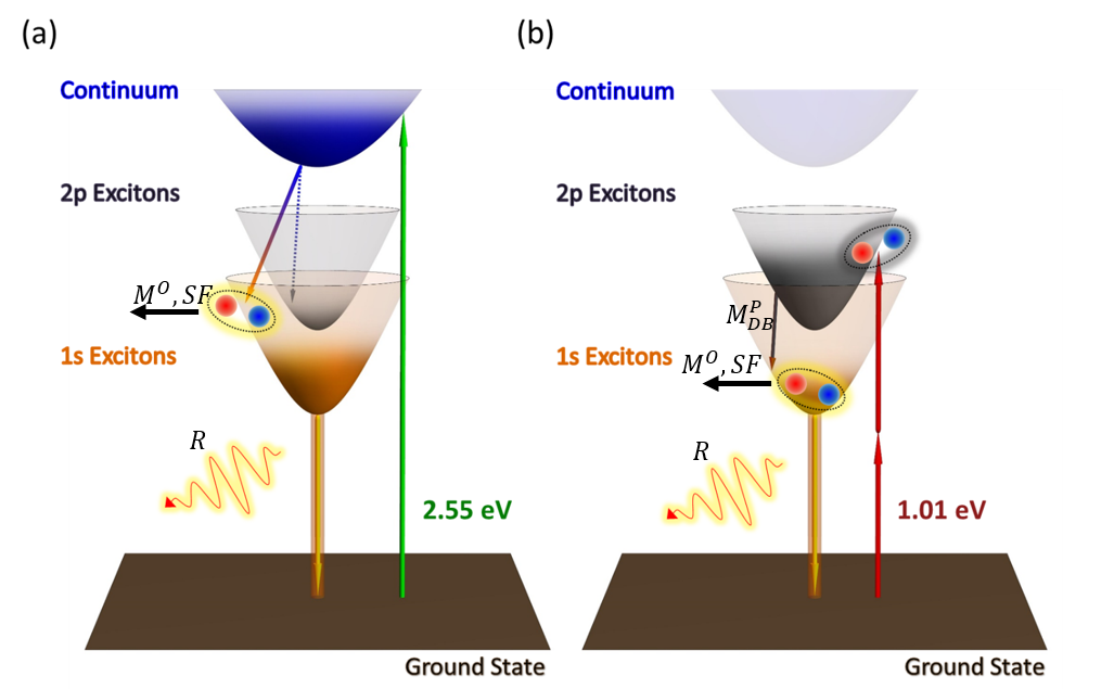
2D Heterojunction Electro-optics
Monolayer 2D materials exhibit a variety of interesting optical properties such as direct band gap, room temperature stable excitons, valley and spin selective excitation, inter-material excitons and many more. Dark excitons are a kind of optically inactive excitions with an order of magniture larger life time useful for memory and storage applications. We will fabricate 2D material heterojunctions and conduct ultrafast measurements at various temperatures.
Low dimensional electron transport
Superconducting interfaces with semiconductors and normal materials have been well studied and mostly understood for both high-Tc and low Tc superconductors. What lies unexplored is the area of superconducting interfaces to 2D materials. Initial theoretical proposals on graphene was made and was found to match with experimental studies. However, even the simplest interfaces with gapped 2D semiconductors such as MoS2 is not been observed yet. There are additional open questions about interfaces of layered 2D superconductors and other materials. Ofcourse, one can also include the surface conductors, topological insualtors, such as the tellurdide and antimonide family.
Two Dimensional Molecular Sieves
Graphene is impermeable to helium. The ultra-thin layer of the graphene sheet makes it an attractive permeation membrane. However the difficulty is in realizing controllable pores. Here, we work with computational folks to design defect structures in large area monolayers and study the molecular dynamics through the engineered holes.
