

Materials for optoelectronic applications have received a lot of attention worldwide in a variety of fields over the past several decades. However, the usual problem of conventional semiconducting optoelectronic materials (viz. metal oxides) is wide bandgap. Thus, it usually absorbs only ultraviolet light and shows almost no response to visible and near infrared light. Hence, doping-mediated modulation of the bandgap is one of the most pragmatic approaches adopted in the pursuit to improve photo absorption properties of conventional wide bandgap semiconducting materials in the visible region. Recently, perovskites have also been revolutionized the field of emerging photovoltaic and optoelectronic technologies. Long diffusion length, high carrier mobility, low recombination rate, strong absorption of light and very cheap manufacturing costs have enabled its success in the field of solid-state photovoltaics.
Understanding this at the theoretical perspective is never been easy because of the exchange-correlation functional that needs to be carefully analyzed in the light of electron's self-interaction error and spin-orbit coupling (SOC). In addition, Density Functional Theory (DFT) with local / semi-local functionals (viz. LDA or GGA), is not sufficient to determine the excited state properties. To circumvent this problem DFT+U and/or hybrid functionals are sometimes effective in determining the structure and energetics of the excited states. However, in many instances these approaches are also insufficient for precisely describing the electronic energy levels. This indeed is the reason behind several controversies between the experimentally and theoretically predicted bandgap, formation energy, concentration and their optical properties.
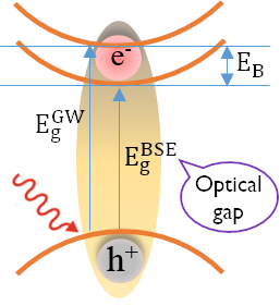
Therefore, to study the optical properties of doped system, we need an advanced computational method, which is reliable enough to evaluate the precise bandgap and excited states. A general framework for the first-principles calculation of excited state properties is provided by many-body perturbation theory (MBPT) approach. These approaches of beyond DFT formalism are essential for a quantitative description of photoemission, inverse photoemission and light absorption experiments in these materials. Therefore, the perpetual growth of modern computing architectures allows us to work on advanced computational method like many-body perturbation theory (MBPT), which includes first order (GW) and higher order Bethe-Salpeter Equation (BSE). This approach permitted us to simulate optical absorption spectra and various properties (viz. refractive index, extinction coefficient, reflectivity, absorption coefficient, loss spectrum etc.) with unprecedented accuracy. We have extensively worked in this field in recent past to address several challenges of capturing excited states physics accurately.
Some of the recent works are mentioned below. For complete list see our publication above:

The intrinsic defects and impurities play an important role on electrical and optical properties of semiconductors. The role of individual defects is important in order to engineer semiconductor materials with specific properties for desired applications. The creation of a defect in the bulk or at the surface of a semiconductor changes the free energy of the system. Depending on environmental conditions viz. temperature, pressure and concentration of doping, formation of defects may be energetically favored for many semiconducting materials. Therefore, in those instances, the defects are inevitable and formation of defects leads to a favorable Gibbs free energy of formation compared to its pristine counterpart.
The Gibbs free energy of formation G (T, p) for an isolated point defect is given by the change in free energy of the system containing the defect at a given charge state with respect to the pristine neutral system. The formation energy depends on the position of the Fermi level, i.e. concentration and type of dopants. In an experimental setup, the position of the Fermi level is often hard to determine accurately and doping or creating non-equilibrium populations of charge carriers by optical excitation can alter its position. Moreover, the free energy of formation of one isolated defect can be reduced significantly by several eVs, when the charge carriers (holes or electrons) are available in the material. Thus, disentangling the relative stability of different types of charged defects in enhancing certain properties is quite challenging. It’s therefore of paramount importance to provide theoretical guidance to experiment about the stability of different dopants as a function of charges at a realistic condition.
We have combined DFT with ab initio thermodynamics to correctly predict the stability and concentration of defects at various materials experimentally relevant temperatures and realistic pressure conditions. We investigate the interplay of bond-making, bond-breaking, and charge-carrier trapping at the bulk and surfaces of various materials including metal-oxides, 2D materials, energy materials, perovskites, topological insulators etc.
Some of the recent works are mentioned below. For complete list see our publication above:

This project is driven by the vision of computational design of functionalized nano-structures. The discovery of the extraordinary activity in catalysis exhibited by small metal-oxide nano-structures (viz. stand-alone clusters or functionalized on top of surfaces) have stimulated considerable research interest to understand the origin of this unusual behavior. It has been found that reducing the number of particles in a cluster reveals the possibility of several interesting size effects. In a range where matter is reduced to sizes of only a few atoms, the intrinsic properties of the so-called functionalized nano-structure are non-scalable from their bulk analogues. These structures exhibit significant variations as a function of size in their physicochemical nature and electronic properties viz. ionization potentials, electronic affinities, hardness, softness, magnetic moments, and catalytic reactivity. Despite significant efforts, the evolving field of heterogeneous catalysis demands the accurate description of all the (meta-)stable structures of the catalyst-materials under operational conditions. In the presence of a realistic reactive atmosphere, clusters change their stoichiometry by adsorbing the ligands from the environment, under certain conditions. This new composition may work as active (functional) material. We have developed various multi-scale-based methodology comprising various length and time scale to address the functional properties of clusters in a technologically relevant atmosphere.
Some of the recent works are mentioned below. For complete list see our publication above:
Since from the discovery of graphene, 2D materials have established a huge sensation both in fundamental research and industrial projects. Theoretical studies on these materials started even before -- and have contributed immensely to the understanding of graphene like layered materials such as silicene, germanene, etc. to transition metal dichalcogenides (TMDs), followed by exfoliation of layers from the bulk structures for instance hematene, which is single layer obtained from hematite (α-Fe2O3). Now, in recent times the focus has been to tune the properties of different 2D materials for specific applications, by doping, strain engineering and van der Waals heterostructures.
2D heterostructures have been studied for varied applications such as p-n and Schottky diodes, field effect transistors, electrode for Li-ion battery, electrocatalysis and photocatalysis. Moreover, the problem of lattice mismatch is avoided in heterostructures as there are no dangling bonds in the constituent layers. There are many factors that govern the properties of the heterostructures, some of them are mentioned as: (a) type of heterostructure (type I, II and III), (b) distance between the layers, (c) commensurate or incommensurate heterostructure, and (d) stacking configuration. The heterostructures with different type of band alignments serve different purpose. Type I (symmetric) band alignment supports efficient recombination, hence, is utilized in LEDs. Type III (broken) band alignment supports the engineering of conduction to valence band transition energy. Type II (staggered) band alignment results in band offsets in either conduction or valence band, thereby confining the carriers. This type is widely used for photocatalytic applications.
Photocatalytic technology addresses the issue of clean sustainable energy as the energy generation process does not add significantly to the pollution, hence being referred as green technology. The utilization of van der Waals heterostructures for photocatalytic reactions requires the analysis of band edge alignment, charge carrier mobility and optical absorption. The heterostructures display band edge levels closer to the requisite condition and helps in reducing e-h recombination rate as e-h separation occurs in two different layers. Since, there are vdW interactions between the layers, the effects due to the hybridized bands will not be significant in the electronic and structural properties, thereby making it easier to project the properties of possible heterostructures by studying the individual properties of the 2D materials. The mix and match approach displays large permutation and combination in designing van der Waals heterostructures. This gigantic pool of heterostructures is an active field of study with varied aforementioned applications.
Some of the recent works are mentioned below. For complete list see our publication above:
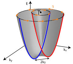
Quantum materials have emerged as the promising materials exhibiting exotic quantum phenomena such as quantum fluctuations, quantum entanglement, superconductivity and topological phases in recent years. These include superconductors, topological insulators, spin-based field effect transistors, multiferroics to name a few. Advanced relativistic quantum mechanical methodologies are needed to explain such behavior in these materials. These class of materials show interesting spin-based splitting that has widely encouraged researchers to understand this spin manipulation. The inversion symmetry leads to Kramers degeneracy in which every band is at least doubly degenerate throughout the Brillouin zone. However, systems without inversion symmetry leads to an interfacial electric field, which lifts the Kramers degeneracy of bands. An electron moving relativistically through this electric field experiences a Lorentz transformed magnetic field given by B=-(vxE)/c2, which interact with electron’s spin moment. This gives rise to several interesting quantum phenomena, which require in-depth analysis of the electronic structure via advanced state-of-the-art theoretical methodologies.
A class of quantum materials is called ferroelectric Rashba semiconductors, where simultaneous occurrence of ferroelectricity and bulk Rashba effect are observed. In ferroelectric Rashba semiconductors, electric control of spin-degree of freedom makes them suitable for spintronics-based devices. The complete reversal of spin-texture on reversing the direction of polarization is of the great importance in this class of materials. We have started working very recently in this field and the first work of our group is referred below.