
Layer Transfer of 2D Materials Using Quasi-Dry
Method
The quality of a synthesized film depends on
various factors, including the choice of substrate for film deposition, what
are the required precursors for growth, growth pressure and temperature, and so
on. Most TMDCs are typically synthesized at temperatures above 500 °C, making
it impractical to deposit on temperature-sensitive substrates. There are
several layer transfer processes to overcome the temperature dependent issues such
as the wet-etching method, water-assisted transfer method, double support
layer-based transfer method, and so on that have been studied and optimized for
two-dimensional (2D) materials in our lab group. Presently, the wet etching
transfer is extensively employed for the transfer of MoS2. The wet
etching method involves applying a layer of polymethylmethacrylate (PMMA) onto
the MoS2 material through spin coating. The PMMA/MoS2
stack is then separated from the substrate using chemical etching, typically
employing hydrogen fluoride (HF) or other strong etchants. However, this
chemical etching process can harm the MoS2 film and degrade its
quality, which is undesirable for the heterostructure formation. Therefore,
there is a strong demand for a highly efficient, repeatable transfer approach
that avoids damage and ensures the preservation of film integrity.
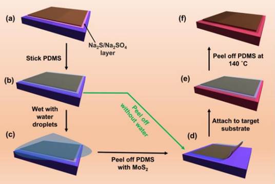
In our lab, we developed a novel transfer
process named the quasi-dry layer transfer method, free from PMMA residues and
chemical etchants. The schematic illustration for MoS2 layer
transfer by this process is shown in Figure 1. Since this layer transfer method
utilizes only PDMS and water, it can be referred to as the quasi-dry layer
transfer method. Furthermore, the quasi-dry layer transfer process has emerged
as a highly versatile technique for creating 2D/2D (MoS2/WS2
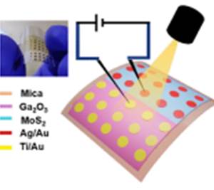
and vice versa) and 2D/3D (MoS2/β-Ga2O3) van der Waals (vdW) heterostructures as shown in Figure 2. We also
fabricated MoS2/mica and MoS2/β-Ga2O3/mica
flexible photodetectors and studied their performance with bending/tensile
strain and temperature. The responsivity and detectivity of the MoS2/mica
flexible photodetector were found to be 1.10 mA/W and 3.86 × 10¹⁰ Jones,
respectively. The PDCR, responsivity, and detectivity of the MoS2/β-Ga2O3/mica
flexible photodetector were calculated to be 103, 7.21
mA/W, and 2.4 × 10¹¹ Jones, respectively. The photocurrent and responsivity
were increased by 155% and 136% under 0.61% tensile strain.
![]()
Figure 1.
Schematic of MoS2 layer transfer by quasi-dry layer transfer process
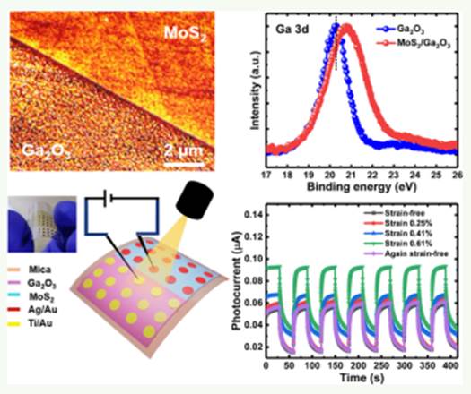
Figure 2. (a) AFM image of
the MoS2/β-Ga2O3
heterostructure, (b) XPS spectra of the Ga 3d core level for pristine β-Ga2O3
and MoS2/β-Ga2O3,
(c) Schematic illustration of the MoS2/β-Ga2O3
flexible photodiode, (d) Time-dependent photoresponse
of the device under different bending states (strain states)
