
Advancements in Material Synthesis via Chemical
Vapor Deposition
The
Chemical Vapor Deposition (CVD) technique plays a pivotal role in the growth of
materials, offering unparalleled control and precision in material synthesis.
CVD allows for the creation of large-area, high-quality materials with
controllable properties, making it indispensable for a wide range of
applications, from cutting-edge electronics and optoelectronics to energy
storage and sensing. Its scalability, versatility in precursor materials, and
ability to fine-tune growth parameters empower researchers and industries to
tailor 2D materials to specific needs. As a cornerstone in the 2D material
synthesis toolkit, CVD contributes not only to the advancement of technology
but also to our understanding of fundamental material science, making it a
crucial technique for unlocking the potential of 2D materials in the modern
world.
Two-dimensional
(2D) materials, such as graphene, transition metal dichalcogenides (TMDs), and
black phosphorus, have emerged as remarkable materials with a wide range of
applications in electronics, optics, energy storage, and more, owing to their
exceptional properties. The synthesis of these materials using Chemical Vapor
Deposition (CVD) techniques is of paramount importance because it enables
precise control over material properties, scalability for industrial
applications, and the creation of large-area, high-quality films.
The
purpose of this report is to highlight the expertise of our laboratory in the
synthesis of materials using CVD techniques. We will describe our experience
and proficiency in this field, demonstrating our ability to harness CVD methods
for the controlled growth of 2D materials. This report serves as a testament to
our capability to produce high-quality 2D materials, which have a promising
future in various technological and scientific applications. In our lab we have
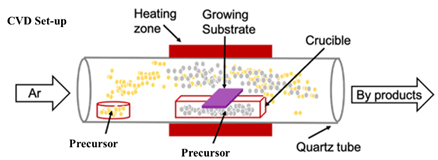
single-zone APCVD system (MTI Corporation, OTF-1200X-S50-2F) and its schematic
is as shown in Figure 1.
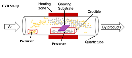
Figure 1 Schematic of CVD set-up
The
early developments in CVD synthesis were done on β -gallium oxide in our
lab. The research conducted by Sudheer Kumar, Vipin Kumar, Trilok Singh, A. Hähnel, and Rajendra Singh
investigates the impact of deposition time on the structural and optical
properties of β-Ga2O3 nanowires synthesized via the
Chemical Vapor Deposition (CVD) technique. While specific details of the
research are not provided, the study likely explores the systematic variation
of deposition times to understand how they affect the crystal structure,
morphology, and optical characteristics of the β-Ga2O3
nanowires. This research aims to provide insights into optimizing the growth
process for tailored properties, which is essential for potential applications
in optoelectronics, sensing, and related fields. By gaining a deeper
understanding of how deposition time influences structural and optical
properties, this study contributes to the knowledge required for the precise
engineering of β-Ga2O3 nanowires with desired
characteristics [1]. Some of their results are listed in Figure 2.
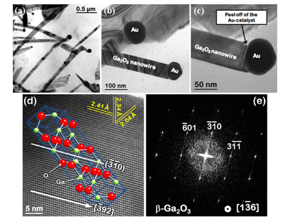
Figure 2 a
TEM image showing the general morphology of b-TEM image showing the general
morphology of β-Ga2O3 nanowires grown using Au
catalyst at 900°C for 4 h, (b–c) TEM images of β-Ga2O3
nanowires at low and higher magnifications, (d) HRTEM image of a single β -Ga2O3
nanowire. The d-spacings between the fringes are marked in the image which is
overlaid with the model of the β-Ga2O3 structure, (e)
Fast Fourier-Transform (FFT) of the single β -Ga2O3
nanowire in (d) specifying the orientation of the wire axis by the streak
In an extended study by Sudheer et
al. on beta gallium oxide (β -Ga2O3)
nanowires (NWs), the growth of these NWs using the Chemical Vapor Deposition
(CVD) technique on different substrates was investigated in our lab. The study
involved the growth of β -Ga2O3
NWs on three different substrates: silicon (Si), sapphire, and GaN/sapphire. Field emission scanning electron microscopy
(FESEM) results showed that the NWs grown on GaN/sapphire
exhibited superior alignment compared to those on the other substrates. The diameter
of the β -Ga2O3
NWs ranged from 150 to 400 nanometers, and they
reached lengths of several tens of micrometers. This
indicates the ability to control the size and length of the NWs during the CVD
growth process. X-ray diffraction (XRD) and high-resolution transmission
electron microscopy (HRTEM) confirmed that the NWs possessed a single
crystalline monoclinic structure. This demonstrates the high-quality
crystalline nature of the NWs. Raman spectroscopy analysis revealed that the
samples had similar Raman spectra with two active modes - mid and high
frequency. Notably, a low-frequency mode was absent in the results. Cathodoluminescence
(CL) spectra of β -Ga2O3
NWs on different substrates showed a strong broad UV-blue emission band and a
weaker red emission band across all the samples. This suggests that the optical
properties of the NWs were consistent, regardless of the substrate used. In
summary, the study found that the morphological and structural properties of β -Ga2O3 NWs
grown on different substrates exhibited some variations, with superior
alignment observed on GaN/sapphire. However, their
optical properties remained quite similar, as indicated by the consistent
UV-blue and weak red emission bands in the CL spectra [2]. These findings
provide valuable insights into the controlled synthesis of β -Ga2O3 NWs for
various applications. The successful growth of gallium oxide was a significant
achievement in our laboratory, demonstrating our proficiency in utilizing the
Chemical Vapor Deposition (CVD) technique for advanced material synthesis.
The
study conducted by Aditya Singh, Madan Sharma and Rajendra Singh focuses on the
NaCl-assisted Chemical Vapor Deposition (CVD) growth of trilayer
molybdenum disulfide (MoS2) and investigates
the role of the concentration boundary layer in 2D material synthesis. They utilized
a two-zone horizontal tube furnace for the CVD process. The precursor for
molybdenum was Mo(CO)6, and sulfur was
introduced in the form of H2S gas. The innovation in this study was
the introduction of sodium chloride (NaCl) as a transport agent. Fine NaCl
powder was employed, which was essential for enhancing the growth of trilayer MoS2. The growth process took place on
SiO2/Si substrates. Various growth parameters, such as temperature
and duration, were systematically varied to understand their effects on MoS2
growth. NaCl acted as a catalyst, promoting the formation of trilayer MoS2 while inhibiting the growth of
monolayer or bilayer MoS2. This selective growth is of paramount
importance as it enables the controlled synthesis of trilayer
MoS2, which is particularly desirable for certain applications,
including optoelectronics. The use of NaCl led to the production of
high-quality trilayer MoS2. The resulting
material exhibited improved properties, making it suitable for advanced device
applications. By adjusting the growth parameters and optimizing the
concentration boundary layer, they successfully achieved the large-area
synthesis of trilayer MoS2[3]. XPS, XRD, TEM
and SAED pattern is shown in Figure 3 which reveals the quality of grown 3L MoS2
film.
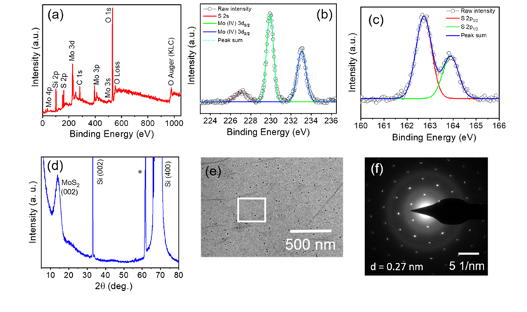
Figure 3 a) XPS survey spectrum of 3L-MoS2.
Core-level XPS spectrum of (b) molybdenum and (c) sulfur.
(d) XRD of 3L-MoS2 grown over the SiO2/Si substrate. (e)
TEM image of 3L-MoS2 and the marked white triangle shows the region
where the SAED pattern was taken and is depicted in (f).
Notably, Aditya Singh et al., as part
of our research team, have also played a pivotal role in extending our lab's
capabilities and expertise to another frontier: the controlled synthesis of
molybdenum disulfide (MoS2) using CVD. Their work represents a
notable accomplishment, providing valuable insights and strategies for
precisely engineering 2D materials, such as MoS2, which is of great
interest due to its exceptional properties and wide-ranging applications. Aditya
Singh and their team have shown remarkable skill and innovation in developing
techniques for the controlled growth of MoS2 via CVD. This accomplishment is of
utmost importance, as the controlled synthesis of 2D materials is a challenging
and critical aspect of modern materials science. By achieving this, they have
unlocked the potential to customize the properties of MoS2 for
specific applications in electronics, photonics, and more. Their contributions
underscore the laboratory's dedication to advancing the field of materials
science and its commitment to staying at the forefront of cutting-edge
research. The insights and strategies provided by Aditya Singh and the team not
only add to the collective knowledge in the realm of 2D materials but also
position our laboratory as a leader in the controlled synthesis of these
materials, fostering innovation and driving the development of future
technologies. This achievement is a testament to the lab's commitment to
excellence and its contribution to scientific progress. The key findings and
advancements in this research are as follows. The study involves a quantitative
comparison of three different precursors for CVD synthesis of MoS2,
namely molybdenum trioxide (MoO3), ammonium heptamolybdate
(AHM), and tellurium (Te) [4]. This comparison
provides crucial information for selecting the most suitable precursor for MoS2
synthesis. Raman spectroscopy as a function of active precursors is shown in
Figure 4. 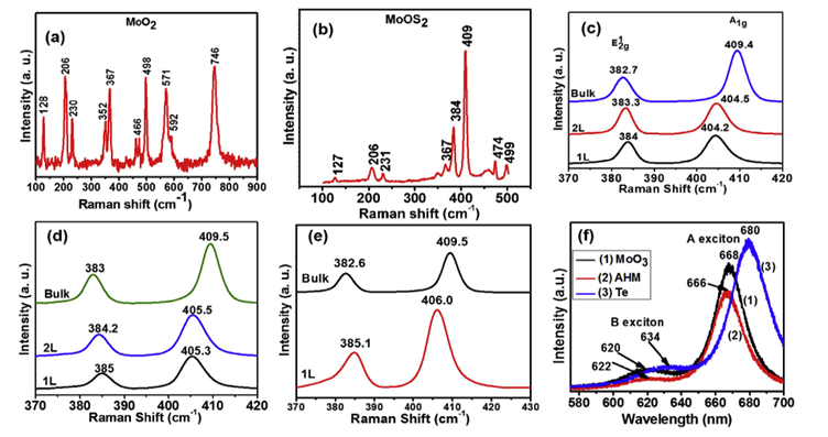
Figure 4 (a) and (b) Raman spectra of micro
particles of MoO2 and MoOS2, respectively. (c) Raman
spectrum of crystalline 1L, 2L, and bulk MoS2 synthesized using MoO3
precursor (d) and (e) Raman spectra of CVD MoS2 synthesized by AHM
powder and Te-assisted growth, respectively. (f) PL
spectrum of MoS2 triangular MoS2 flakes grown via a
different combination of precursors. PL spectrum (1), (2), and (3) correspond
to MoS2 synthesized by MoO3, AHM and Te
assisted, respectively. In all these three PL spectrums, higher and lower
energy peak corresponds to B exciton and A exciton, respectively.
Further,
the research is carried forward by Pallavi et al., who represent a significant
advancement in the synthesis of large-area monolayer tungsten disulfide (WS2)
using atmospheric-pressure Chemical Vapor Deposition (CVD). This work delves
into the growth mechanism and the influence of various parameters, including
the use of NaCl as a growth promoter, sulphur quantity, temperature, gas flow
rate, and hold time. Through the examination of optical microscope images,
Raman, and photoluminescence spectra at different synthesis parameters, the scholars
provided valuable insights into the WS2 film's growth process. The
AFM and HRTEM data shown in Figure 5 confirm the successful large-area growth
of monolayered WS2 film is achieved.
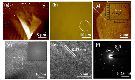
Figure 5 (a) AFM image of the region
highlighted in Figure 4a. Triangular stacks indicate island growth. (c) AFM
image of the large-area monolayer WS2 film shown in (b). A line
profile spectrum is taken along the dashed line. (d) Low-resolution HRTEM image
of the freely suspended film on a TEM grid. The inset of the image shows the
FFT pattern, and the hexagonal arrangement of dots represents its six-fold
symmetry. (e) Zoomed-in HRTEM image of the region shown in (d) (f) SAED pattern
of the freely suspended film on a TEM grid
Furthermore,
they successfully fabricated photodetectors with high responsivity and specific
detectivity in both the visible and ultraviolet regions, demonstrating the
material's potential for UV-visible photodetection applications. This work
showcases the significance of controlled synthesis techniques for enabling
large-area production of 2D materials with tailored properties and their
subsequent application in advanced photodetection
technologies [5].
The
prospects of 2D materials synthesized using CVD techniques by our lab hold
great promise for advancing future electronics. By tailoring the properties and
quality of 2D materials, we can contribute to the development of ultra-thin,
high-performance transistors, sensors, and photodetectors, enabling more energy-efficient
and faster electronic devices. This innovation has the potential to
revolutionize the electronics industry and drive the creation of
next-generation technologies.
References
1. Kumar,
S., Kumar, V., Singh, T., Hähnel, A., & Singh, R.
(2014). The effect of deposition time on the structural and optical properties
of β-Ga2O3 nanowires grown using CVD technique.
Journal of nanoparticle research, 16, 1-9.
2. Kumar,
S., Tessarek, C., Christiansen, S., & Singh, R.
(2014). A comparative study of β-Ga2O3 nanowires
grown on different substrates using CVD technique. Journal of alloys and
compounds, 587, 812-818.
3. Singh,
A., Sharma, M., & Singh, R. (2021). NaCl-assisted CVD growth of large-area
high-quality trilayer MoS2 and the role of
the concentration boundary layer. Crystal Growth & Design, 21(9),
4940-4946.
4. Singh,
A., Moun, M., & Singh, R. (2019). Effect of different precursors on CVD
growth of molybdenum disulfide. Journal of Alloys and Compounds, 782, 772-779.
5. Aggarwal, P., Kaushik, S., Bisht, P., Sharma,
M., Singh, A., Mehta, B. R., & Singh, R. (2022). Centimeter-scale
synthesis of monolayer WS2 using single-zone atmospheric-pressure
chemical vapor deposition: a detailed study of parametric dependence, growth
mechanism, and photodetector properties. Crystal Growth & Design, 22(5),
3206-3217.
