
Our group focused on the Fabrication of Schottky
barrier diodes on β-Ga2O3 and studied the effect of
harsh environments such temperature, gamma-irradiation, swift heavy ion
irradiation on electrical performance of these Schottky barrier diodes. β-Ga2O3
with superior material properties like ultrawide bandgap ~4.9 eV, high BFOM and
JFOM, high thermal and chemical stability emerged as potential candidate for
next generation power electronics especially Schottky barrier diodes and field
effect transistors. Along with excellent material properties, the availability
and ease of growth of high-quality low cost single crystalline wafer up to 6 inch
dia. have been demonstrated by melt growth techniques such Czochralski, edge defined
film fed growth etc., which further enables the growth of high quality
homoepitaxial thin film by various thin film growth methods such as halide
vapor phase epitaxy (HVPE), molecular beam epitaxy (MBE), metal-oxide chemical
vapor deposition (MOCVD). This is a huge advantage over other commercialized
wide bandgap semiconductors like SiC and GaN and makes possible future mass
production of β-Ga2O3 power devices. Controllable
n-type conductivity has been also achieved using Si, Sn as dopant in range of
1016 – 1020 cm‒3 which enable flexibility
for device engineering.
Vertical Schottky diodes on β-Ga2O3
by utilizing whole wafer volume and without affecting chip area offered high
current density and high breakdown voltage capabilities. For high performance
of Schottky diodes on β-Ga2O3, apart from high
quality wafer; high thermal stable Metal-semiconductor contacts: Ohmic contact
and Schottky contact, and repeatability is critical.
In this Direction we are fabricating Schottky diodes
on HVPE-grown β-Ga2O3 (001) epilayers using various
Schottky contacts such as Ni, Pt etc. These Epilayers were grown on high
conductive EFG-grown β-Ga2O3 substrates. Fabricated
SBDs exhibited high rectification ratio of order of 1012 at room
temperature, and we observed breakdown voltage greater than 200 V with high
Schottky barrier heights greater than 1 eV and near unity ideality factor.
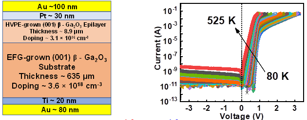
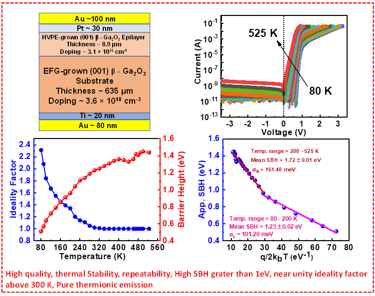
We reported the temperature endurance capability of
high-quality Pt-based Schottky Barrier Diodes (SBDs). The measurements have
been performed over a wide temperature range of 80–525 K, and the prepared SBDs
showed outstanding thermal stability over repeated cycles of electrical
measurements. At higher temperatures, a near unity ideality factor was
observed, which was attributed to the dominance of pure thermionic emission
current transport mechanism at higher temperatures. SBH (ϕ)C–V calculated
from the capacitance-voltage characteristics were found to decrease with
increasing temperature, and their temperature coefficient values of −3.74
to −7.29 × 10⁻⁴ eV/K were observed, which can be attributed to the
narrowing of the bandgap of β-Ga2O3 with the
increase of temperature. A negligible value of intrinsic carrier concentration
below 300 K and a low value of the order of 10−5 – 10−6 cm−3
at room temperature was also calculated from the temperature-dependent C-V
characteristics, which indicated the excellent quality of HVPE-grown Si-doped
(001) β-Ga2O3 epilayers.
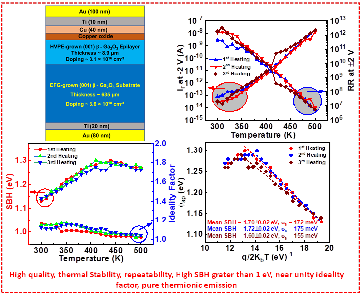
We
proposed the use of Cu as the alternative of Ni and Pt to fabricate SBDs on β-Ga2O3. The fabricated SBDs using Cu as
Schottky contact exhibited high performance. A high Schottky barrier height
(SBHs) with values greater than 1.0 eV, near-unity ideality factors, and a high
rectification ratio (RR) of 1012 at 300 K were observed.
Temperature-dependent current-voltage (I–V–T) and capacitance-voltage (C–V–T)
measurements were performed multiple times in the temperature range of 300 K –
500 K. The SBHs (ϕ)IV calculated from the IVT characteristics
initially increased with temperature and then decreased with near-unity
ideality factors. The increase in (ϕ)IV with temperatures up to
410 K indicated the spatial inhomogeneity at the metal-semiconductor interface.
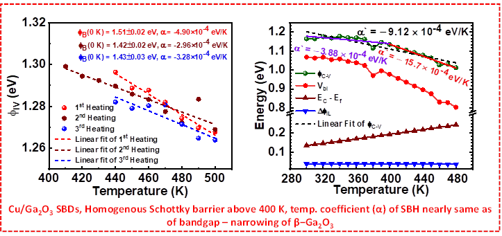
The observed decrease in (ϕ)IV above 410 K showed the
enhancement of barrier homogeneity at higher temperatures (⩾410 K). The reduction in (ϕ)IV above 410
K and decrease in (ϕ)CV calculated from the CVT
characteristics, with increasing temperature, were assigned to the bandgap
narrowing of β-Ga2O3. The IVT measurements were
repeated many times, and the SBDs exhibited excellent thermal stability and
showed high SBHs >1.0 eV, a high RR, and near‒unity ideality factors.
All these findings were attributed to the formation of a high-work-function
copper oxide thin film at the interface between Cu and β-Ga2O3.
These findings allowed fabricating a Schottky contact with a high and
homogeneous barrier and thermal stability using cheap, abundant Cu material,
enabling low-cost mass production of future power semiconductor devices based
on oxide semiconductors.
References
1. Hardhyan
Sheoran, and Rajendra Singh, Investigation of high-performance Schottky
diodes on a Ga2O3 epilayer using Cu with high barrier
height, high temperature stability and repeatability. Journal
of Physics D: Applied Physics, 2023.
2. Hardhyan
Sheoran, Janesh K. Kaushik, and Rajendra Singh, Study of electrical
characteristics of high quality Pt SBDs fabricated on HVPE-Grown β-Ga2O3
epilayers in a wide temperature range (80–525 K). Materials
Science in Semiconductor Processing, 2023.
3. Hardhyan
Sheoran, Vikram Kumar, and Rajendra Singh, A Comprehensive Review on Recent
Developments in Ohmic and Schottky Contacts on Ga2O3 for
Device Applications. ACS
Applied Electronic Materials, 2022. (Review Article)
4. Hardhyan Sheoran, Bhera Ram Tak, N. Manikanthababu, and Rajendra Singh, Temperature-Dependent Electrical
Characteristics of Ni/Au Vertical Schottky Barrier Diodes on β-Ga2O3
Epilayers. ECS
Journal of Solid State Science and Technology, 2020.
