
![]()
Ultra-Wide
band Gap (UWBG) Solar-Blind Photodetectors
Modern day technologies are seeing a huge thrust in
the development of smart materials and devices. These materials and devices
have qualities such as lightweight, transparency, robustness, flexibility,
environmentally friendliness, and lowcost and enrich human
life with advanced functionalities. Besides the smart functionalities, various
flexible sensors can be useful for healthcare as well.
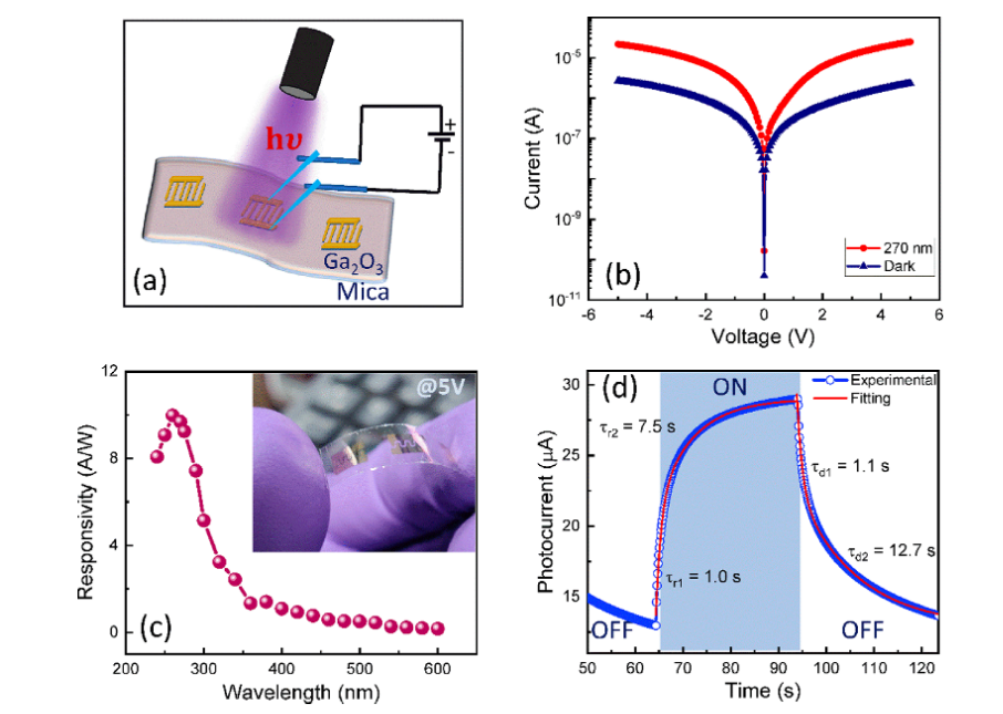
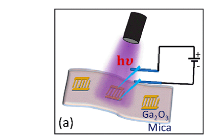
The
ultrahigh photoresponsivity of 9.7 A/W is obtained
for 5 V applied bias at room temperature under 75 μW/cm2weakillumination
of 270 nm wavelength. The detector enables very low noise equivalent power
(NEP) of 9×10⁻¹³ W/Hz1/2 and ultrahigh detectivity
of 2×10¹² jones which shows the magnificent detection sensitivity.
Further, bending tests are performed for robust utilization of flexible
detectors up to 500bending cycles with each bending radius of 5 mm. After 500
bending cycles, the device shows a slight photocurrent decrease. The bending
performances exhibit excellent potential for wearable applications. Moreover, photocurrent
and dark current characteristics above room temperature demonstrate the
outstanding functionalities until 523 K temperature, which is remarkable for
flexible photodetectors. The obtained results show the potential of gallium
oxide solar-blind photodetectors at room-temperature and high-temperature
environments, paving the way for futuristic smart sensors.
Deep Ultraviolet
Detector on mica substrate (Ram et. al 2019)
Deep ultraviolet photodetectors (DUVPDs) (<280nm),
also known as solar-blind PDs, have piqued interest due to their wide range of
applications in defence, space communication, civil, agriculture, healthcare,
UV astronomy, high-temperature flame detection, solar-blind imaging for missile
tracking, ozone hole monitoring, and other fields. Wide-bandgap and
ultrawide-band-gap semiconductor materials such as GaN,
AlGaN, diamond, Lu2O3, and Ga2O3have emerged as
promising candidates for solar-blind PDs because of their wide- and
ultrawideband gap due to which they exhibit intrinsic solar-blindness. Unlike
commercially available UVPDs based on narrow-band-gap semiconductor materials
such as Si and GaAs, they do not require any additional optical filter or large
cooling systems.
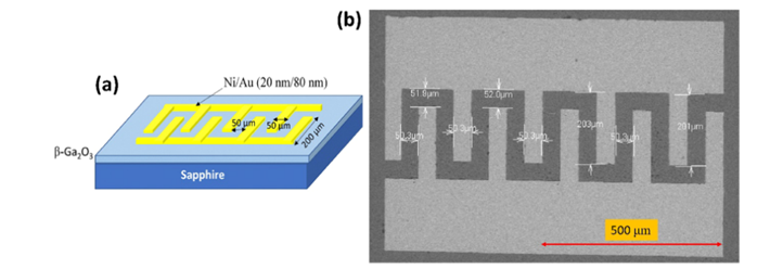
Here in our work, we have grown thick gallium oxide
incorporated with buffer layer of gallium oxide to maintain high quality of
crystallinity on the sapphire by the MOCVD, the fabricated the device through
the lithography followed by metallization. The performance of device in
summarized way
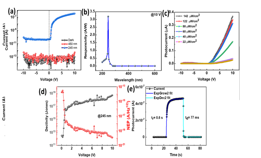
ultra-high-performance DUV PDs based on UID
MOCVD-grown β-Ga2O3were fabricated, and the gain and the self-powered behavior were thoroughly investigated. The high-temperature
stability of DUV PDs on films up to 125°C was demonstrated. The dark current was
observed to be extremely low and found to be almost constant across the whole
temperature range. The UV−visible (260:500nm) rejection ratio was found
to be >103 at zero bias and >105 at higher biases, and
it increased with the rise of temperature. All other performance parameters of
PDs remained at high values throughout the entire temperature range. The
Schottky barrier height lowering effect caused by an induced electric field and
localized self-trapped holes at Ni/β-Ga2O3interfacewere attributed to the
gain mechanism. The self-powered behavior of PDs was
attributed to the barrier inhomogeneity at the Ni/β-Ga2O3interface.
Schematic of the
Ga2O3 Device (Hardhyan et. al.
2022)
The Dynamic
temporal temperature-based performance. (Taslim
et.al.)
The use of 2D
materials as potential substitutes for conventional 3D electrical connections has
grown considerably in recent years. These materials have special benefits, when
used to create van der Waals (vdW) heterojunctions.
These heterojunctions are not obligated to conform to the strict requirements
for lattice matching and processing compatibility that are present in
conventional bonded heterojunctions, and there is no chemical reaction taking
place at the interface, as opposed to while metal contacts with semiconductors
react to produce oxide and nitrides. Traditionally only metal and oxide
electrode have been utilized in in device fabrication Ag, Graphite, Ni/Au,
Pt/Au, Cr/Au, Ti/Au, ITO, IZO and IGZO.
