
Computing devices built on von Neumann architecture suffer
from “memory wall” problem, often known as the von Neumann bottleneck
limitation which leads to temporal latency, high power consumption, and a high
risk of data loss while handling enormous amounts of data resulting in reduced
data bandwidth. Brain inspired neuromorphic computing is an emerging
technological application which requires handling of massive amount of data
along with high clocking speed, making devices based on von Neumann architecture
unsuitable. To circumvent this challenge, modern day computing devices follow
processing-in-memory (PIM) architecture which fuses the memory module with CPU
to reduce or eliminate the frequent data transmission. Memristors enable true
PIM as a fundamental device which supports both storage and data computation.
Memristor is a two terminal device non-volatile memory
device whose resistance can be precisely modulated depending upon the history
of electrical current passed through it. Human brain is composed of 1011
neurons which are interconnected through 1015 synapses. Biological
neurons play a crucial role in processing signals related to the reception,
integration, and transmission of sensory and perceptual information. These
neurons encode information through action potentials, which are electrical
signals in the form of spikes. Neurons collect input signals from pre-neurons
through their dendrites. Subsequently, the integrated signals in the soma
trigger output signals, which are transmitted along the axons to post-neurons
when the sum of input signals surpasses a certain threshold. The biological
synapse, found between a neuron's axon and dendrite, facilitates the
transmission of signals. The metal electrodes in memristors can be visualized
as the pre- and post-synaptic neuron, while the channel separating them as the
synaptic cleft. Therefore, like synapse, electric signal transferred through
the device can be controlled through its resistance.
Memristors have been classified under four categories
depending upon their operation mechanism:
1. Ionic Migration, where a material is sandwiched between two metal
electrodes and the resistive switching occurs due the formation of a conducting
filament between the active metal electrodes. Their operation can be explained
through electrochemical metallization (ECM)or through valence change mechanism
(VCM).
2. Phase Change, where phase transition of the switching material governs
the switching mechanism, and the device is composed of a phase change material
sandwiched between two metal electrodes.
3. Spin, where a non-magnetic layer
is sandwiched between two ferromagnetic layers. Here, the relative direction of
magnetization of these ferromagnetic layers governs switching mechanism.
4. Ferroelectric, which follows metal/ferroelectric-film/metal device
architecture. Here, polarization of charges in the ferroelectric film governs
the switching behaviour.
Memory-intensive applications also demand high density
device integration, which necessitates a nano-scale downscaling of the devices'
dimensions. To address this issue, 2D materials are being investigated for low
power memory device applications.
Rhenium Disulphide (ReS2) is a layered semiconducting group
VII TMDC exhibiting distorted 1T’ crystal structure. Weak interlayer bonding,
soft Re-S bonds, and high probability of sulfur vacancies due to their low
forming energy makes ReS2 a potential material for non-volatile
resistive switching (NVRS) device application.
Our research group specializes in manufacturing
memristors using chemical vapor deposition grown 2D thin films. In our lab, we
conducted experiments on a CVD grown ReS2 film to assess its suitability for
resistive switching device applications. We investigated the impact of various
metal electrodes (Pt/Au and Ag/Au) as well as different channel widths (200, 100,
and 50 μm). The observed resistive switching behavior in devices with
Ag/Au electrodes was attributed to the Electrochemical Metallization (ECM)
mechanism, whereas in devices with Pt/Au electrodes, it was ascribed to
defect-mediated charge transport. (https://doi.org/10.1039/D3NR02566G)
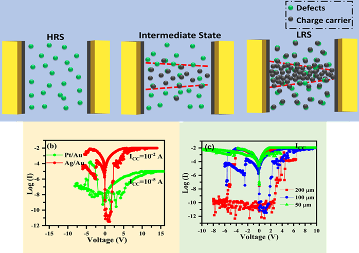
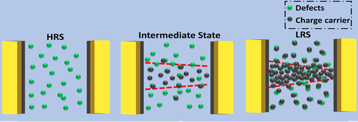
Figure: (a) Schematic
depicting the formation of conducting filament due to movement of metal ion and
defect mediated charge carrier transport. (b) Comparative RS cycle of memristor
with Ag/Au and Pt/Au electrode. Ag/Au showed 105 times higher ION/IOFF
ratio and reason is attributed to electrochemical active nature of Ag
electrodes. (c) I-V curve depicting the effect of channel width (200, 100, and
50 µm) on memristive behaviour. Highest switching ratio for 50 µm is attributed
to the ease of formation of CF due to reduced distance between the metal
electrodes.
