
Wide Band Gap Quantum Emitters
Quantum dots have been extensively studied as
potential single photon sources for quantum computing. However, the use of
quantum dots for quantum computing applications is hindered by various limitations,
including low brightness, spectral instability, and environmental sensitivity.[1]
Therefore, in our lab we intend to explore the
potential of widebandgap materials like AlN and hBN quantum emitters. They
have a broad transparency window covering from ultraviolet to mid-infrared, and
a significant second-order nonlinear optical effect.[2] Since they are
wide-bandgap material, it makes it chemically and mechanically robust material
that is stable under a wide range of environmental conditions, including
temperature, humidity, and light exposure. Above and beyond, the
size and shape of AlN and hBN
quantum emitters can be controlled with high precision using modern
nanofabrication techniques, such as electron beam lithography and dry etching.
This allows for the fabrication of uniform and reproducible quantum emitters,
which can lead to improved device performance and industrial scalability.
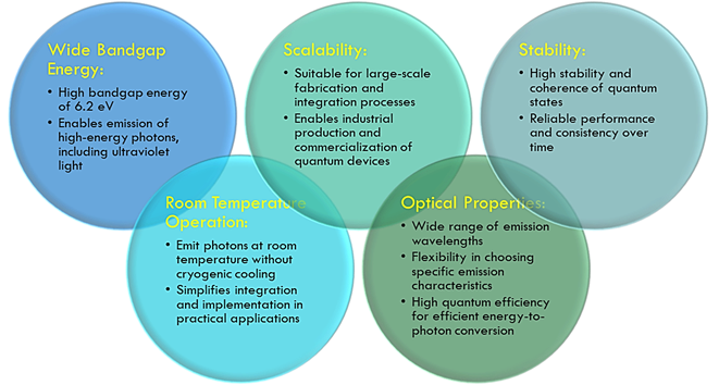
Figure
1: AlN and hBN
quantum emitters exhibit a wide-bandgap, high thermal conductivity, and strong
piezoelectric effects, making them highly efficient and versatile for quantum
applications
AlN Quantum emitters:
In
our lab we fabricate AlN epitaxial film using MBE, MOCVD
system in collaboration with SSPL Delhi which has large bandgap of 6.2 eV,
with a wide transparency window and a significant second-order nonlinear
optical effect. This enables the AlN-based photonics
devices to work in UV, visible, near-infrared (NIR) and up to MIR wavelength
regime. Theoretical calculations have shown that AlN
can serve as a stable environment for hosting well-isolated quantum emitters.
This makes AlN quantum emitters less sensitive to
external factors. Also, this property leverages its suitability for integration
with existing electronic devices, such as transistors and sensors for practical
applications. Apart from that, its fabrication process is monolithically compatible with
CMOS fabrication line, which enables the wafer-level fabrication of AlN-based integrated photonics devices with low cost and
high reliability. Compared with other
semiconductor materials (e.g. Si, Ҡ = 145 W/(m·K)), AlN has significantly higher
thermal conductivity (Ҡ = 285 W/(m·K)), which can help dissipate heat generated during
operation, reducing the risk of thermal damage to the device. Also, AlN has small thermo-optic coefficient (dnAlN/dT = 4.26 × 10⁻⁵/K
at 1000 nm). These thermal properties make AlN-based
devices able to handle high optical power since it is more tolerable to
temperature fluctuations. Despite their promising characteristics, to fully
harness AlN quantum emitters for quantum technologies
further research is necessary to fully unlock their potential. Notably, the
identification and characterization of the point defects responsible for
quantum emission in AlN stand as a significant
knowledge gap. Therefore, in our lab we intend to assess the potential of AlN quantum emitters in achieving high-fidelity quantum
operations.
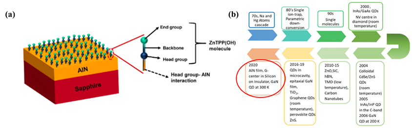
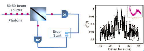
Figure 2: (a) AlN epitaxial
film (1μm thick) grown over sapphire by physical vapor deposition (b) Recent
review article showing AlN quantum emitters are a cutting-edge technology to
create chip-scalable quantum emitters
hBN Quantum Emitters:
Hexagonal boron nitride (hBN) is a layered two-dimensional (2D) material similar
to graphene. Unlike graphene, which is considered semimetal, hBN is an
ultra-wide band gap semiconductor with a bandgap of ~6 eV. Because of its high thermal and chemical stability,
hBN
is used as an encapsulator. Recently it has been
found that hBN
has luminescence emission in FUV (far ultraviolet), UV (ultraviolet), and
visible range. Thus, hBN
has potential applications as a light-emitting diode in the FUV region.
In our lab, we use mechanical exfoliation method to prepare hBN samples. We perform various treatment to activate
defects in hBN. These defects inherit the property of
2D quantum emitters. Different characterization techniques such as Atomic Force
Microscopy (AFM), Raman Spectroscopy, Field Emission Scanning Electron
Microscopy (FESEM), and Energy Dispersive X-Ray Analysis (EDX) have been
utilized to study the morphology and chemical composition of hBN flakes.
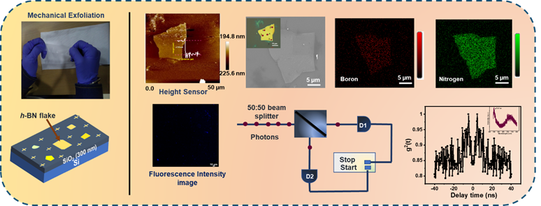
Figure 3: Here in our lab we mechanically exfoliate the h-BN
flakes from bulk and study various characterization techniques for quantum
emitter applications
[1] F. P. García de Arquer, D. V. Talapin, V. I. Klimov, Y. Arakawa, M. Bayer, and E. H. Sargent, "Semiconductor quantum dots: Technological progress and future challenges," Science, vol. 373, p. eaaz8541, 2021.
[2] T.-J. Lu, B. Lienhard, K.-Y. Jeong, H. Moon, A. Iranmanesh, G. Grosso, et al., "Bright high-purity quantum emitters in aluminum nitride integrated photonics," ACS Photonics, vol. 7, pp. 2650-2657, 2020.
