2D Quantum materials form a category of ultrathin
(atomic scale) materials that exhibit many exotic fundamental properties due to
the strict confinement of carriers in one dimension, such as high carrier mobility,
tunable bandgap, strong spin-orbit coupling, large magnetoresistance and high
excitonic binding energy. Graphene, being the first and most intensively
researched material of this category, has paved the way for various other
quantum materials such as hBN, black phosphorus, and
different types of metal chalcogenides. Transition metal dichalcogenides
(TMDCs) are this category's second most probed materials after graphene owing
to their diverse optical, electronic, superconducting, and topological
properties. In addition to these fundamental properties, stacking the same or
different 2D materials provides another degree of freedom for tuning their
properties, thus making it one of the potential categories of materials for future
digital and quantum device applications.
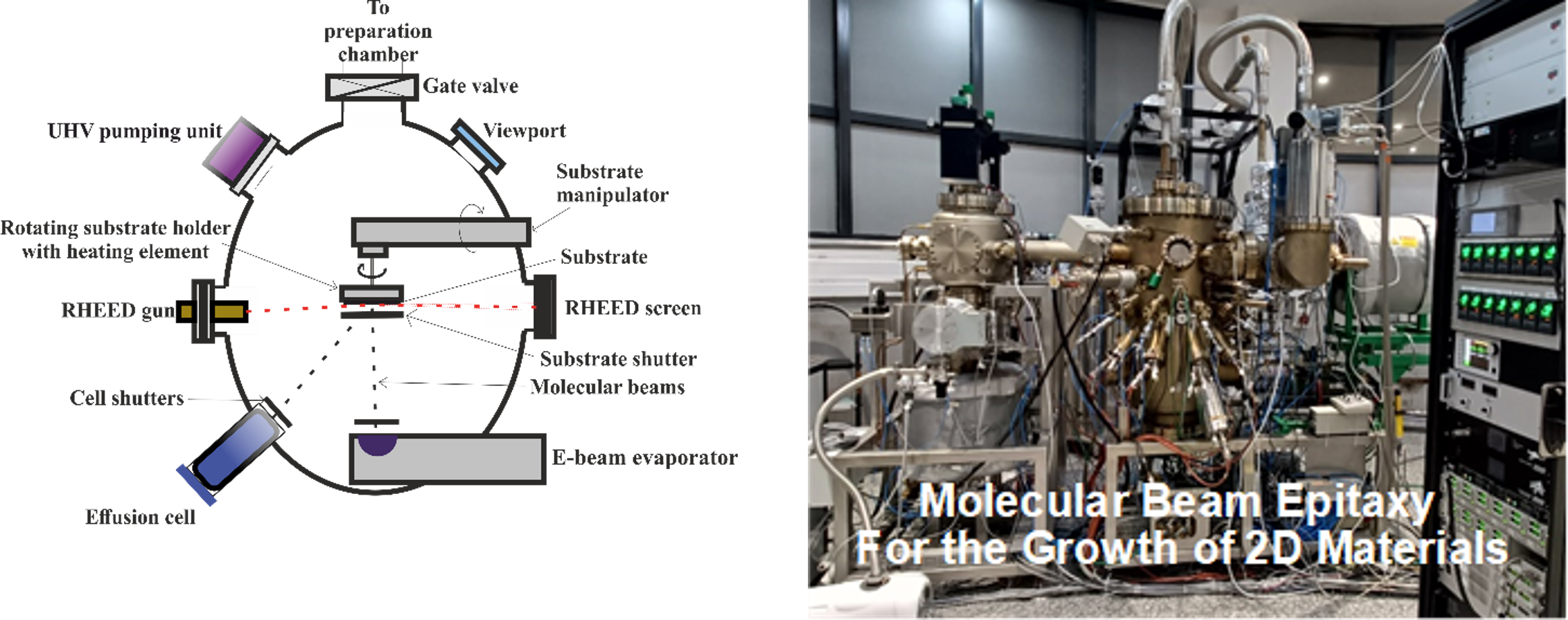
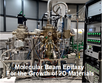
Molecular
Beam Epitaxy (MBE) is one of the sophisticated techniques for the growth of
high-quality 2D materials. It employs molecular beams of source material to
deposit on the heated substrate under an ultra-high vacuum (UHV) environment
with base pressure ~10-10–10-11 mbar to produce high-quality
epitaxial 2D films. Unlike some other techniques, the use of UHV and high-purity
elemental material sources leads to extreme cleanliness of the grown 2D
material. The use of individual shutters for each material cell and small
precursor fluxes lead to precise control over the amount of depositing material
and, thus, the film thickness (down to a single monolayer), making MBE one of
the important techniques for realizing vertical heterostructures.
One
of the most potent aspects of MBE is its ability to monitor the details of the
growth precisely and simultaneously, with the help of different in-situ
facilities and characterization techniques such as quartz crystal microbalance
(QCM) for measuring real-time thickness and growth rate, reflection high-energy
electron diffraction (RHEED) for observing the film quality, growth orientation
as well as the growth rate, spectroscopic ellipsometer for the optical
properties and layer thickness; most of which necessarily require a high level
of vacuum for their smooth operation, hence benefit from the UHV environment
inside an MBE system.
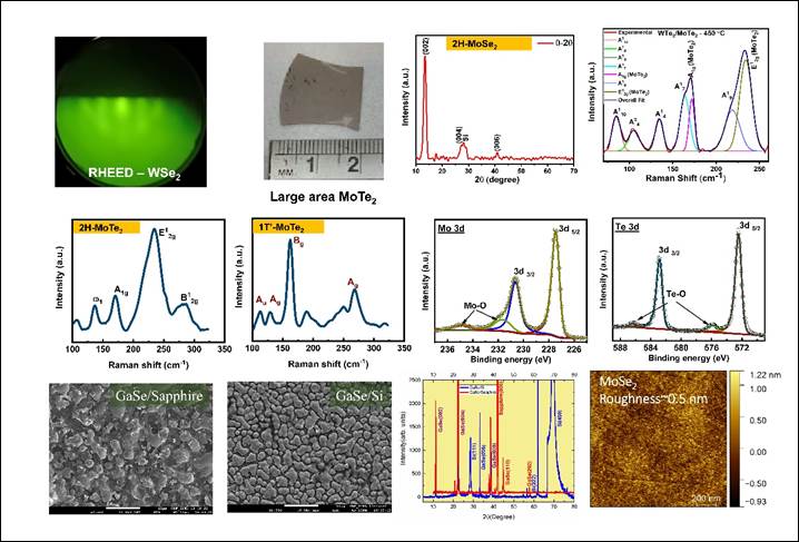
Our
group focuses on the growth of the following large area and high-quality,
few-layer thick 2D TMDC materials using molecular beam epitaxy. The growth is
optimized for different materials to achieve a pure phase of a particular
material. Various characterization techniques, as shown in the figure below,
have been utilized for investigating different properties of the grown
ultrathin films.
Materials
grown using the 2D MBE:
·
MoTe2 on
silicon and sapphire
·
MoSe2 on
silicon and sapphire
·
WSe2 on
silicon and sapphire
·
GaSe on silicon and
sapphire
·
WTe2 on
Sapphire and MoTe2/sapphire
·
GaTe
on sapphire